
Micron's G11 NAND: Wafer bonding and 400-plus layers target late 2027 launch
The memory maker plans to double density to 42 Gb/mm2 and cut power consumption by 25% using a manufacturing process already employed by rival YMTC.
By Megan Greco ·
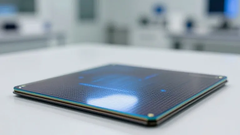
Micron Technology plans to begin mass production of its next generation 3D NAND flash, designated G11, in the second half of 2027. The company outlined the specifications at an event this week, positioning the new memory as a major step forward in storage density and efficiency. The launch follows a period of intense competition among memory manufacturers seeking to meet rising demand for high-capacity solid-state drives.
The G11 architecture relies on wafer-on-wafer bonding to achieve its performance targets. This technique allows Micron to fabricate the NAND array and the peripheral circuitry on separate wafers, optimizing each for its specific function before joining them. Scott DeBoer, the company's president and chief technology and products officer, stated that the timing is right for this approach. He described the new product as the world's most advanced NAND, confirming the use of the bonding method previously adopted by Chinese rival YMTC.
Micron projects that G11 will double the storage density of its current G9 generation. The new chips are expected to reach approximately 42 Gb/mm2 in triple-level-cell form, up from about 21 Gb/mm2. The design will also feature faster input and output speeds, rising from 3,600 MT/s to 5,400 MT/s. This increase in throughput is intended to support both traditional data center storage and emerging artificial intelligence workloads that require high bandwidth.
Energy efficiency will improve alongside speed. Micron estimates that the energy required to transfer each bit will drop by more than 25 percent. The company has not disclosed the exact number of memory layers in G11, but confirmed the design will exceed 400 active wordlines. The density gain comes from a combination of increased layer counts and a smaller memory cell pitch, which Micron describes as industry-leading.
The move places Micron ahead of its competitors in near-term density metrics. Rival firms such as Kioxia and Samsung have announced next-generation products with lower density targets. Micron officials said they will share more technical details as high-volume production approaches next year. The company also indicated it is developing new high-mobility materials and denser cell architectures for future generations, aiming to scale in all three dimensions rather than relying solely on layer counts.
Source: Tom's Hardware