
Four Masks Push Chinese Chipmakers Past the Cost of the Banned EUV Tech
Morgan Stanley reports that CXMT yields are one-third lower than Western peers as manufacturers stack extra exposure steps to bypass EUV restrictions.
By Chloe Zhao ·
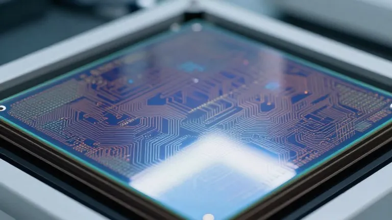
Morgan Stanley estimates that Chinese DRAM maker CXMT produces only about one-third as many bits per wafer as its Western competitors. This efficiency gap stems from export controls that keep ASML's extreme ultraviolet lithography machines out of China. Domestic manufacturers must rely on older deep ultraviolet equipment, requiring multiple exposures to print critical layers on silicon.
The multiple patterning technique allows chipmakers to split complex designs into simpler patterns and build them up step by step. Chris Mack, co-founder and CTO of semiconductor firm Fractilia, noted that industry standards previously held that three exposures on a 193 immersion tool cost roughly the same as one EUV exposure. However, at four masks, the cost of the workaround begins to exceed the price of the banned technology.
Quality control presents a secondary challenge. Each additional pattern must align precisely with previous etches, increasing accumulated overlay errors and process variation. Designers often add space around features to compensate, which enlarges the chip and reduces the number of dies per wafer. Mack emphasized that manufacturers sell die, not wafers, making the loss of usable space a direct financial hit when wafers cost tens of thousands of dollars.
SMIC has used this approach to advance its processes without EUV. A 2023 teardown of the Huawei Mate 60 Pro revealed its Kirin 9000S processor was made using a second-generation 7nm-class process. More recent analysis of the Kirin 9030 suggests SMIC has moved its DUV-based process closer to 5nm density, though it still trails leading processes from TSMC and Samsung. Mack cautioned that node labels like 5nm or 3nm have limited meaning without context, and SMIC's N+3 process remains less scaled than established Western equivalents.
The DUV approach still has potential limits. Micron developed its 1-alpha DRAM without EUV, and Morgan Stanley considers CXMT's planned move to 1-alpha DRAM for HBM3e achievable through similar means. Copenhagen Business School researcher Douglas Fuller expects advanced packaging to allow firms to use DUV for the latest DRAM generations by the end of the decade. Mack added that China could progress further if it had a full 193 immersion ecosystem, noting that memory fabrication is easier than logic.
Morgan Stanley projects that CXMT will lift its share of global DRAM bit supply from 14% in 2026 to 16% in 2028 by adding new greenfield capacity. The bank also expects China's AI chip self-sufficiency to rise from 42% in 2025 to 70% by 2030. This growth will occur despite a persistent gap in EUV, HBM, and advanced software.
Source: Tom's Hardware
More Business · Tech news · Bad Business · Report a business · Got a Story?